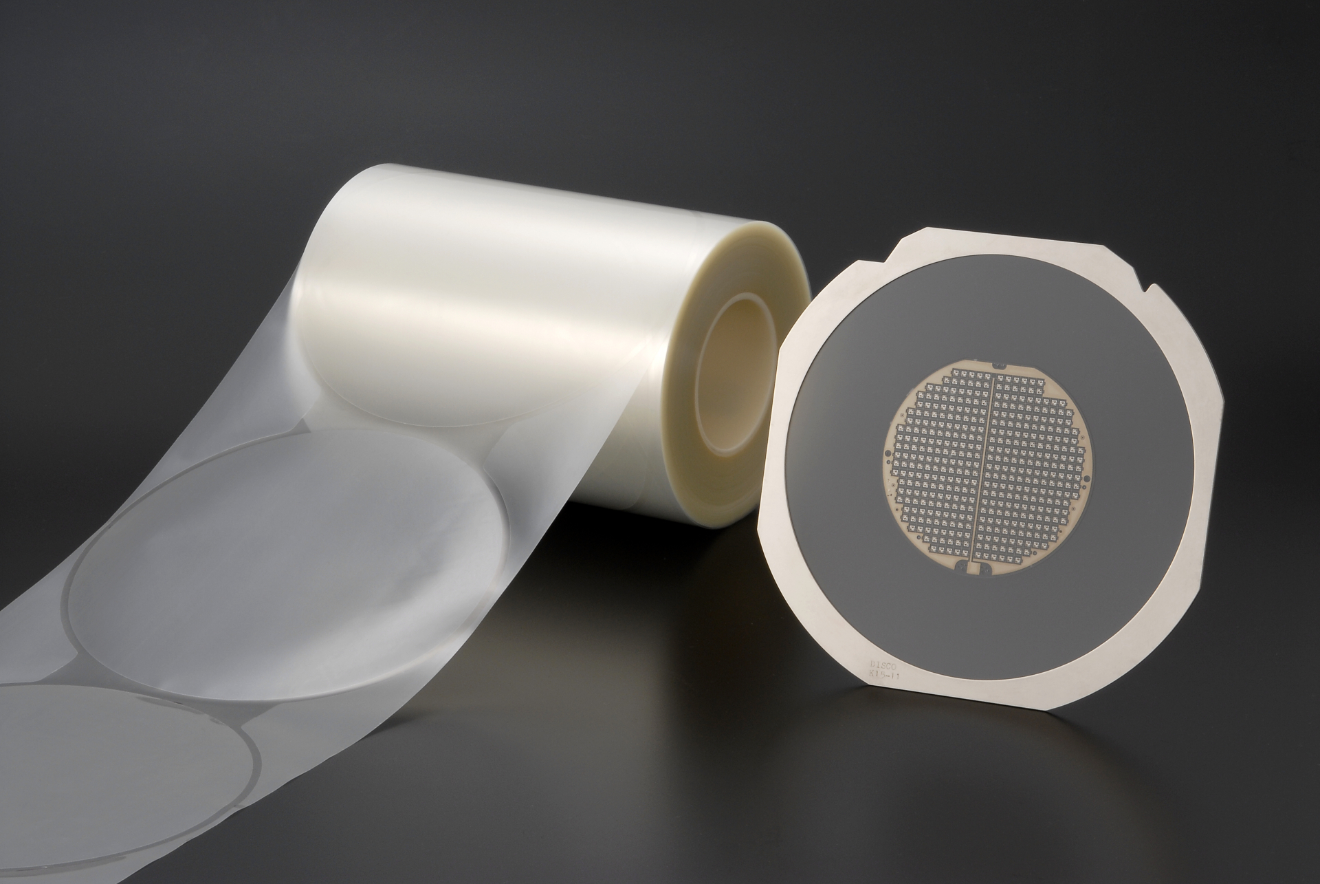
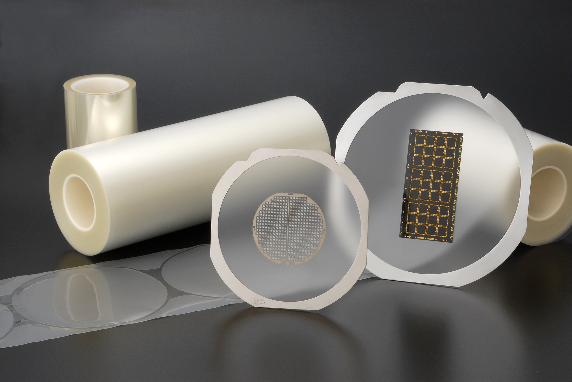


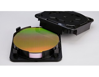
Supporting Semiconductor Manufacturing Processes with Diverse Products
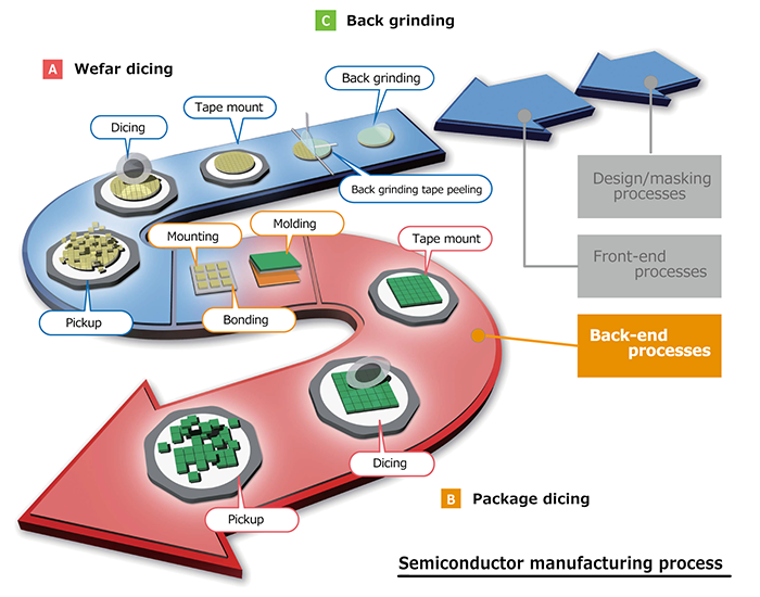
With the recent miniaturization of various electronic devices and the growing demand for semiconductor chips, the needs for various process technologies are growing more and more. In addition, with the ultra-thin wafers brought about by technological innovation, the ability to respond to the back grinding and dicing processes is also in question. Maxell offers solutions suitable for various processes, such as backgrinding and dicing, in the semi-conductor manufacturing process.


Our adhesion test is based on JIS Z 0237(2022).
For comparison to the conventional method, the tested value by Sliontec Method is also described in the parenthesis.

| Model | Product | Application | Features | Tape thickness | Adhesion | Coating |
|---|---|---|---|---|---|---|
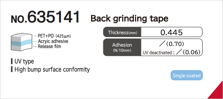
| No.635141 | Back grinding tape | For various back grinding | UV type, High bump surface conformity | 0.445mm | Initial: 0.70N/10mm After UV:0.06N/10mm |
Single |
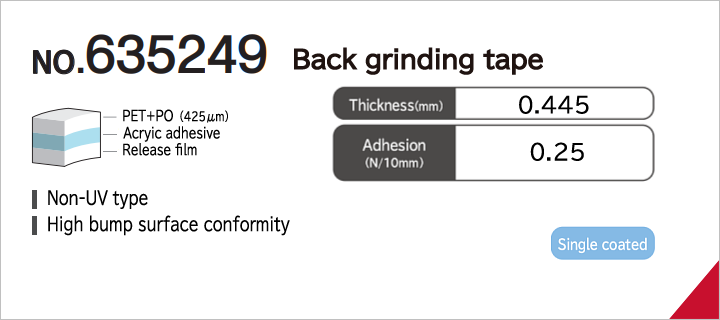
| No.635249 | Back grinding tape | For various back grinding | Non-UV type, High bump surface conformity | 0.445mm | 0.25N/10mm | Single |
| No.636000 | Dicing tape | For various wafer dicing | Standard type | 0.10mm | Initial: 2.80N/10mm After UV:0.23N/10mm |
Single |
| No.636020 | Dicing tape | For various wafer dicing | High fixing force | 0.10mm | Initial: 3.30N/10mm After UV:0.30N/10mm |
Single |
| No.636050 | Dicing tape | For various wafer dicing | Easy pick up | 0.10mm | Initial: 2.80N/10mm After UV:0.08N/10mm |
Single |
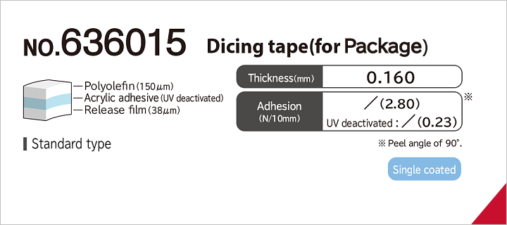
| No.636015 | Dicing tape | For various package dicing | Standard type | 0.16mm | Initial: 2.80N/10mm After UV:0.23N/10mm |
Single |
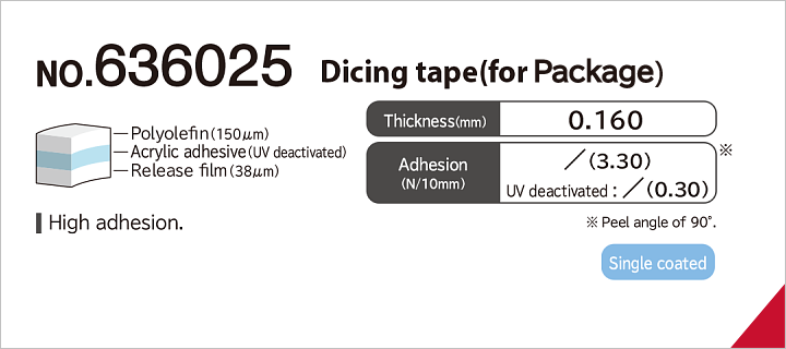
| No.636025 | Dicing tape | For various package dicing | High fixing force | 0.16mm | Initial: 3.30N/10mm After UV:0.30N/10mm |
Single |
| No.636055 | Dicing tape | For various package dicing | Easy pick up | 0.16mm | Initial: 3.00N/10mm After UV:0.10N/10mm |
Single |
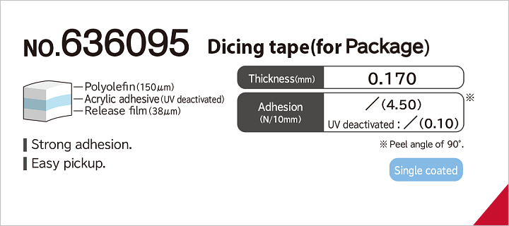
| No.636095 | Dicing tape | For various package dicing | Easy pick up, Strong adhesion | 0.17mm | Initial: 4.50N/10mm After UV:0.10N/10mm |
Single |
Reviews Tapes for semiconductor manufacturing process
Bạn chưa đánh giá sao cho sản phẩm này
Đánh giá ngay